
MIT researchers, together with collaborators from Harvard University, Rice University, Yale University, MIT Lincoln Laboratory and Pohang University in South Korea, have developed a technique that uses graphene to grow air-stable, wafer-scale monolayer superconductors, addressing a longstanding barrier to using these ultrathin materials in practical quantum computing hardware.

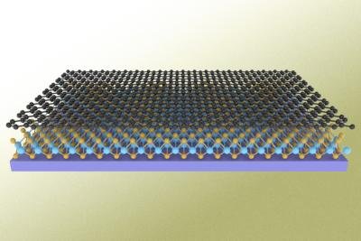
The superconducting material (yellow/blue) grows in the tiny gap beneath a graphene layer (grey) placed atop a silicon dioxide substrate (purple). The graphene shields it from oxidation while guiding it into a smooth, uniform film over a large area. image credit: MIT
Two-dimensional superconductors are attractive for quantum circuits because their compact size and high crystallinity could enable far smaller quantum devices. However, they degrade almost immediately when exposed to air. Niobium diselenide (NbSe2), a monolayer superconductor with especially high kinetic inductance – a property that lets it store large amounts of inductive energy in a very small area – has been particularly difficult to work with at scale: researchers have had to rely on small flakes produced by exfoliation, since large-area growth attempts oxidize and degrade before they can be protected.
The team developed what it calls “encapsulation epitaxy” to solve this problem. Rather than growing the superconductor first and adding a protective layer afterward, the researchers place a layer of graphene on a silicon dioxide substrate before introducing the niobium diselenide precursor materials. The weak adhesion between graphene and the substrate leaves a gap less than 1 nanometer thick, and the niobium diselenide crystallizes within that gap – the substrate traps the precursors long enough for crystal formation to begin, while the graphene layer lets the material spread into a smooth, continuous monolayer. Because the film is already encapsulated by graphene as it forms, it can be moved out of its growth environment into ambient air without oxidizing.
Using this method, the team grew monolayer NbSe2 films larger than 1 inch across. The graphene/NbSe2 heterostructures showed a superconducting transition temperature (Tc) of approximately 1 K and an enhanced charge density wave transition temperature of approximately 177 K. The researchers also developed an oxidation-free transfer technique and a superconducting edge-contact method to integrate the material into working superconducting circuits, where it maintained a measured kinetic inductance of approximately 0.7 nH per square – suitable for quantum circuit elements that require high kinetic inductance.
“Emerging superconductors that are only a monolayer thick have a lot of potential. Thanks to our new process, they are no longer materials that can only be made at a very small scale. There are now exciting opportunities for scientists to study these materials, utilize them in circuits, and explore their practical applications,” said Xudong Sheldon Zheng, a graduate student in MIT’s Department of Electrical Engineering and Computer Science and co-lead author of the study.
Co-lead author Sameia Zaman, also an EECS graduate student at MIT, pointed to the range of directions the work opens up: “We’ve taken a very good step toward exploring both the physics and the application side of this thin, monolayer superconductor, which we can now grow in wafer scale or in even larger areas. There are a lot of directions we can go in the future.”
The researchers say the growth strategy is not limited to niobium diselenide and can be extended to a broader family of monolayer quantum materials. Beyond superconducting quantum circuits, the team points to potential applications in ultrasensitive quantum detectors for communications and cosmology.