
Two-dimensional (2D) superconductors are intriguing platforms for quantum science and many-body physics. They also have flat, crystalline surfaces, which are perfect for dense superconducting circuits. However, producing large-scale monolayer 2D superconductors is difficult because they oxidize in air.
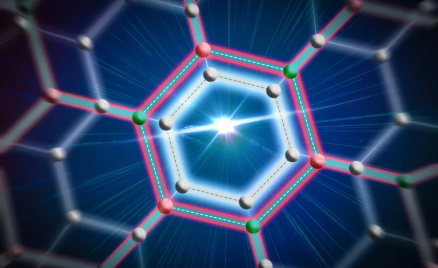
MIT researchers and collaborators have developed a way to create large, uniform sheets of ultrathin superconducting material that remain stable in air. They grow niobium diselenide beneath a protective layer of graphene. The graphene shields the fragile superconductor from oxidation while guiding it to form a smooth, wafer-scale layer.
The researchers incorporated their air-stable superconductor into a microwave circuit and observed that it retained its superconducting state with an impressive amount of kinetic inductance, which is useful for quantum components. This progress may help miniaturize quantum computing hardware and also enable ultrasensitive detectors useful in communication and cosmology.
Co-lead author Xudong Sheldon Zheng said, “Emerging superconductors that are only a monolayer thick have a lot of potential. Thanks to our new process, they are no longer materials that can only be made at a very small scale. There are now exciting opportunities for scientists to study these materials, utilize them in circuits, and explore their practical applications.”

Niobium diselenide is an ultrathin superconductor made of a single layer of niobium atoms sandwiched between selenium atoms. It has very high kinetic inductance, meaning it can store a lot of inductive energy in a tiny area, a valuable trait for quantum devices.
Normally, scientists achieve this by linking many Josephson junctions, but thin niobium diselenide could replace those with a compact film. The problem is that the material quickly oxidizes in air, making it hard to grow large, uniform sheets.
Researchers usually protect it with another 2D layer like graphene or boron nitride, but because oxidation begins almost immediately after synthesis, this protection is difficult and requires strict inert conditions.
MIT researchers took a new approach: they first placed a graphene layer on the silicon dioxide substrate, then grew niobium diselenide in the tiny gap between them.
The substrate holds the precursors long enough for crystals to form, while graphene helps them spread into a smooth monolayer. Using this method, the team produced a perfectly uniform sheet of niobium diselenide over an inch wide. Because the material grows inside the gap and is already encapsulated by graphene, it can be safely removed into air without degrading.
Using the right surface, the MIT team was able to safely transfer their graphene–niobium diselenide structure without oxidizing it and then bond that structure into a quantum circuit while maintaining its delicate characteristics. They etched the edges of this 1-nanometer-thick film in a vacuum not only to deposit it but also to make reliable electrical connections at its edge, smooth as butter.
The material kept its superconducting properties and high kinetic inductance after fabrication, making it ideal for compact quantum devices. The growth method also works for other monolayer quantum materials, opening the door to new physics studies and advanced technologies.
“We’ve taken a big step toward exploring both the science and applications of wafer-scale monolayer superconductors, which we can now grow in wafer scale or in even larger areas. There are a lot of directions we can go in the future,” says co-author Zaman.
Journal Reference:
- Zheng, X., Zaman, S., Zhang, K. et al. Encapsulation epitaxy of air-stable 2D superconductors for quantum circuits. Nature (2026). DOI: 10.1038/s41586-026-10865-1