
Researchers have developed a method that can generate a large, uniform area of ultrathin superconducting material that remains stable in air.
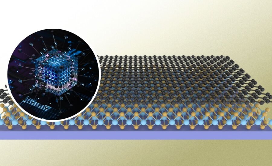
In this effort, researchers involved from MIT and other places grew the superconducting material, called niobium diselenide, underneath another atomically thin material, carbon-based graphene.
The graphene layer protects the fragile superconductor from oxidation, while guiding it to grow in a smooth layer over a large wafer-scale area, according to researchers.
Material maintained its superconducting properties, exhibited high kinetic inductance
Xudong Sheldon Zheng, a graduate student in the MIT Department of Electrical Engineering and Computer Science (EECS) and the co-lead author of this study revealed that emerging superconductors that are only a monolayer thick have a lot of potential.
“Thanks to our new process, they are no longer materials that can only be made at a very small scale. There are now exciting opportunities for scientists to study these materials, utilize them in circuits, and explore their practical applications,” said Zheng.
The research team revealed that they further integrated this air-stable superconductor into a superconducting microwave circuit. When tested, the material maintained its superconducting properties and exhibited high kinetic inductance, which is a resource for many quantum devices.
Ultrathin superconductor composed of single, closely packed layer of niobium atoms
In the long run, this advance could help miniaturize superconducting quantum computing hardware, as well as technologies like ultrasensitive quantum detectors for communications or cosmology. Niobium diselenide, an ultrathin superconductor composed of a single, closely packed layer of niobium atoms sandwiched between a single layer of selenium atoms on either side, has a very high kinetic inductance, as members of the research team recently reported, according to a press release.
This enables the material to store a great deal of inductive energy in a very small area. Large kinetic inductance in a small form-factor is a desirable design element in many quantum devices, according to researchers.
Published in the journal Nature, the study reveals an ‘encapsulation epitaxy’ mechanism that enables the growth of large-area (more than 1 inch), air-stable, monolayer niobium diselenide (NbSe2) films (1L-NbSe2) and explore their potential for superconducting quantum circuits.
This work represents a distinct growth phenomenon in which a 2D encapsulation layer, such as graphene or hexagonal boron nitride, pre-deposited on a 3D substrate (for example, SiO2 or Si3N4) simultaneously serves as a template for the epitaxial growth of 1L-NbSe2 underneath it at the encapsulation–substrate interface and as a protective capping layer against ambient degradation, according to the study.
“Typically, once we make the material and remove it from its inert environment, it immediately starts to oxidize and degrade, ultimately becoming damaged,” Zheng explains.
If scientists could incorporate materials such as thin niobium diselenide with sufficiently large kinetic inductance into a quantum circuit, they could replace the large area of electronic junctions with a tiny piece of thin-film material, making the circuit more compact. But because niobium diselenide degrades rapidly in air, scientists have not been able to reliably fabricate devices at the wafer scale. Instead, they rely on exfoliation techniques that yield small flakes, as per the release.